Constructive principle
An electron microprobe is an electron microscope “enhanced” with 4 – 5 Wavelength Dispersive Spectrometers (WDS) designed for quantitative, non-destructive x-ray microanalysis of solid materials. It is capable of high spatial resolution and relatively high analytical sensitivity. The principle of the EPMA method is very similar to the principle of the Scanning Electron Microscope (SEM) method when it comes to generating X-rays and images. The difference comes when a quantitative analysis is done by the microprobe. The spectrometers are designed and installed in such a way that specific X-rays of selected elements can be “filtered”, counted, and quantified. To achieve this, the detector inside each spectrometer is installed within a certain exact geometry which requires that 1) the sample, 2 ) the X-ray detector, and 3) the analyzing (mobile) crystal inside the spectrometer, always stay on a circle (Rowland circle) of precise radius (140 mm for JEOL, 160 mm for CAMECA).
How does an electron microprobe work?
In an electron microprobe, a solid sample placed in a vacuum is bombarded with a focused beam of high-energy (accelerated) electrons (accelerating voltage 5 – 30 keV). This bombardment results in a variety of interactions between the beam electrons and the atoms and their electrons in the sample (Figure 1). These interactions happen in a very small volume of the sample (100 nm3 to a few µ3, depending on the application), making the microprobe a perfect tool for “in situ” quantitative analysis.
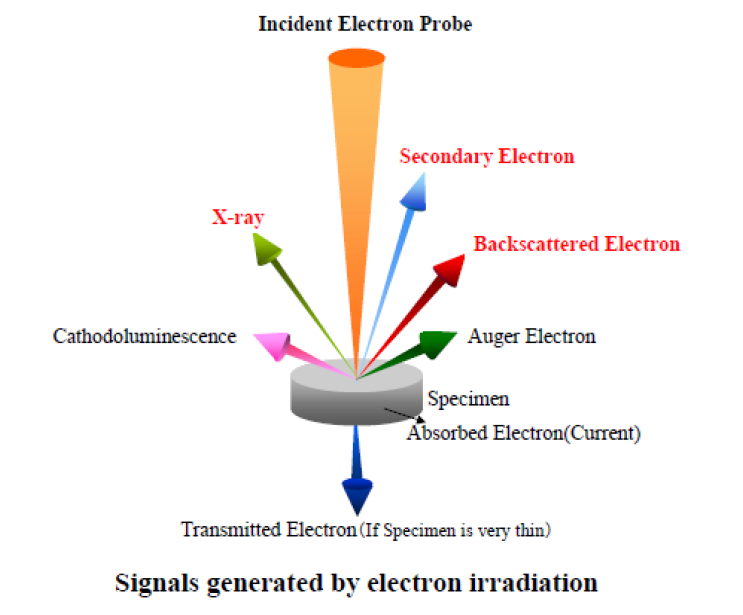
Figure 1. Signals generated by electron irradiation
Some of these interactions produce signals that can be detected and used to provide images, such as Secondary Electron (SE) or BackScattered Electron (BSE) images. Other interactions are used to provide information about the composition of the material being examined. The most important of these interactions is when a beam electron collides with an atom in the sample and causes an inner shell electron (from the K orbital) to be ejected (scattered away) from the atom. The inner shell vacancy leaves the atom in a high-energy excited state. The atom loses this excess energy by “jumping” of an outer shell electron (e.g. from the M orbital) to fill the inner shell vacancy. This jump (transition) is accompanied by the release of a photon. The frequency of this photon emission has a specific wavelength, which is characteristic for an element, and it is the range of X-rays, therefore we can say that an X-ray is produced. As the electron from the outer shell “jumped” to fill in the vacancy in the inner shell, the atom will again remain with a vacancy in the outer shell (e.g. M orbital). Another electron, from an outer shell (e.g. L orbital) will “jump” to fill in the vacancy in the M orbital. Again, this electron jump would create a high-energy state of the atom, and in order to fix this, the atom will emit another photon (X-ray). As it is a continuous bombardment with accelerated electrons, the sample will continuously emit photons (or X-rays) as explained above. The emitted photon has energy equal to the difference in energy between the two shells involved in the transition. For a given transition between a specific outer and inner shell, the energy of the emitted x-ray photon will uniformly increase with increasing atomic number (Z) of the excited atom. This happens because the increase in the positive charge of the nucleus with atomic number causes the electrons in all shells to be bound more tightly and thus have higher energy as Z increases. For a given transition (e.g. electron jumps from L to K orbital), each element will produce x-rays with a unique (characteristic) energy and wavelength. In a graph showing the intensity of the X-rays on “y axis” vs the energy (or wavelength) on “x axis”, a vertical line would correspond to each characteristic X-ray peak. It is these “characteristic x-ray lines” that the electron microprobe uses to identify and quantify the elements present in the sample.
Signals and their use
X-ray lines – identification of elements and quantitative analysis
The electron shells of an atom are labeled K, L, M, N, and O starting with the innermost (lowest energy) shell. These shells correspond to orbitals with principal quantum numbers n=1, 2, 3… (i.e. s,p,d,f,… in quantum notation). For example, the innermost shell of an atom (the K shell) has a complete configuration if it has two electrons. The next shell (L) has a complete configuration with 8 electrons. Unlike in the Bohr’s model of the atom, each of the 8 electrons from L shell vibrates on its own orbit, having little energy differences between each other. One can notate these energy levels as L1, L2, L3…L8. The same applies for the other outer shells (M, N, O). The transitions giving the x-ray lines most often used in electron microprobe analysis (examples in Figure 2) are the transitions L3 – K and L2-K (the Kα1 and Kα2 lines), M5 – L3 (the Lα line), and N7 – M5 (the Mα line) (i.e. in quantum notation 2p3/2 – 1s1/2, 3d5/2 – 2p3/2, and 4f7/2 – 3d5/2 respectively). If the transition is from the M shell directly to the K shell, the X-ray produced is a Kβ. If transition from N to L, then the X-ray is Lβ.
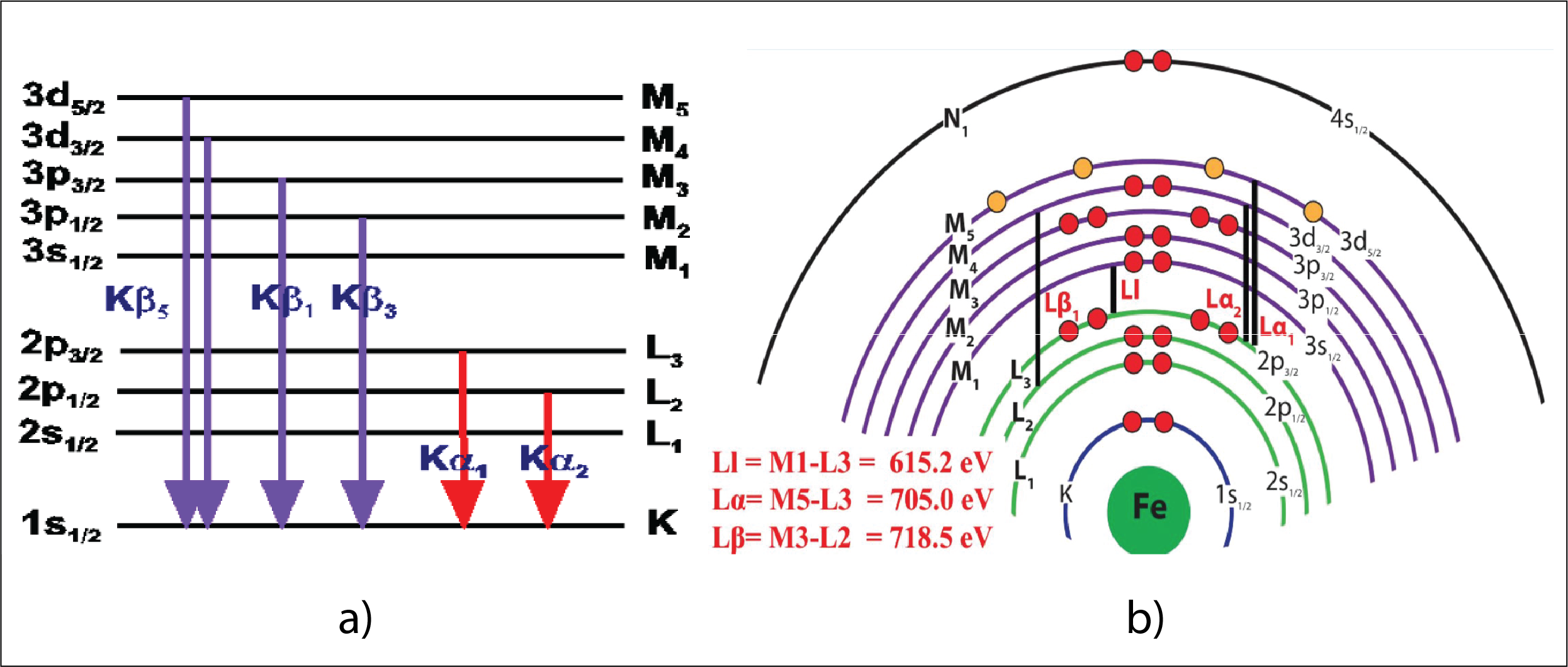
Figure 2: a) Examples of energy transitions and X-ray notation; b) Energy transitions and X-ray examples from Fe (iron)
The characteristic X-rays of the element “i” (Kα, Mα, Mβ… etc.) from an unknown sample are “filtered” with the analyzing crystals (situated inside the spectrometer of the microprobe), then counted by an X-ray detector (also side the spectrometer) to produce an electric signal. This signal is proportional to the number of X-rays which is also proportional to the concentration of the element “i” in the sample. The electrical signal is then amplified and compared to the signal produced in the same conditions by a known standard. The final concentration of the element “i” in the sample is calculated based on the proportionality between the X-ray intensity in the unknown sample and the X-ray intensity produced by the known standard, following a correction procedure to minimize the “matrix” effect on the measurement.
Note: Atoms (elements) are directly detected and measured but not compounds (e.g. molecules as oxides, etc.). E.g. From the measurement of the concentration (wt. %) of element “i” in an unknown silicate, knowing the valence of the element “i”, the result can be calculated and reported as ”oxides”.
X-ray analytical volume and the penetration depth
The analytical volume and the penetration depth of the incident electrons depend on the accelerating voltage and the density of the analyzed material. The higher the accelerating voltage, the bigger the analytical volume and the depth of penetration. The higher the density of the sample, the lower the analytical volume and the penetration depth. By changing the accelerating voltage, the EPMA operator can change the penetration depth for a certain material. The equation linking the accelerating voltage and the penetration depth is given by Castaing’s formula, below.
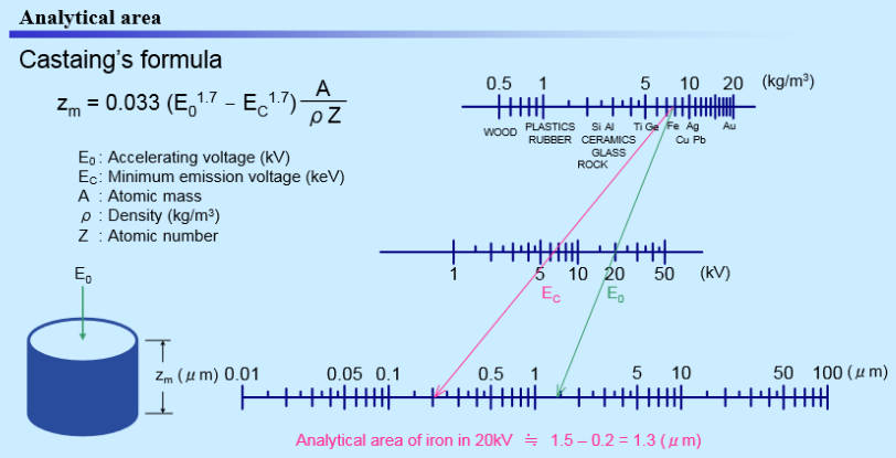
Figure 3. Castaing’s formula to calculate the analytical area, and a graphical scale to estimate the penetration depth as a function of accelerating voltage and the density of the sample.
Backscattered Electrons (BSE) – compositional image
One of the most useful signals of the interaction between the electron beam and the sample is the production of backscattered electrons (BSE). A backscattered electron is a beam electron (not an orbital electron from the sample!) whose trajectory escaped knocking other particles (electrons from the sample). However, its trajectory is deflected by coulombic interactions with the nucleus by elastic scattering events (the electron is turned around and emerges from the sample surface with relatively high energy). The number of backscattered beam electrons is strongly dependent on the average atomic number (Z) of the atoms in the sample. By rastering, the electron beam over the sample surface and having a backscattered electron detector placed near the top of the sample chamber and, it is possible to produce a composition map of the sample’s surface. On the BSE image, the areas with heavier atoms (higher Z) will show brighter, and the areas with light atoms will show darker. Various phases with different average atomic numbers will show different shades of gray. BSE images are extremely useful in analyzing multiphase samples.
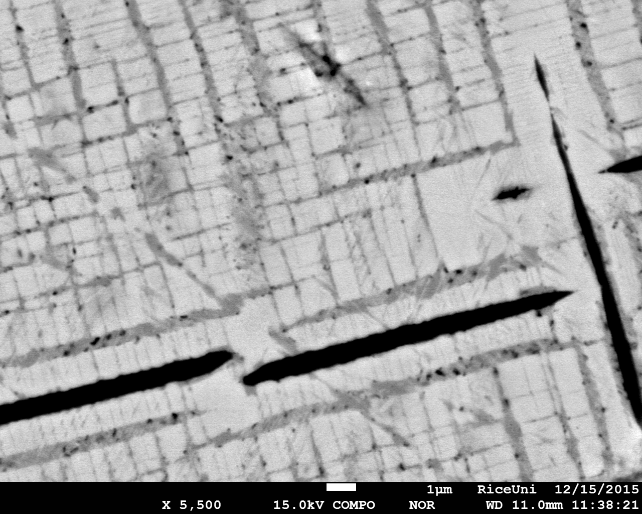
Figure 4. Back scattered Electron image of Ti-rich magnetite with exsolutions of ilmenite (light gray) and spinel (black).
Secondary Electrons (SE) – high-resolution image of the sample’s surface
Another useful signal is produced by inelastic scattering events. If the accelerated beam electron knocks out one electron from the atom “i” in the sample, the energy is partially transferred from the beam electrons to the knocked-out electron. This type of interaction can cause loosely bound electrons of the sample atoms to gain enough energy that they can move through the sample. These electrons are called “secondary electrons” and they originate from the sample (are not deflected beam electrons!). These secondary electrons (SE) have such low energy that only those produced very near the surface can escape the sample and be detected. As a result, secondary electrons can be used to produce high-resolution images of the sample surface that are used in electron microscopy.
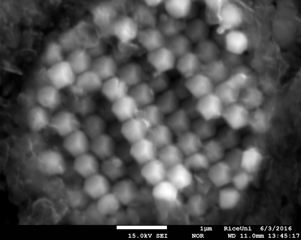
Figure 5. Secondary Electron Image of framboidal pyrite (dodecahedrons of FeS2 nanocrystals) in a black shale
Background Radiation (Bremsstrahlung)
Some of the accelerated beam electrons will be decelerated when they encounter the coulombic field of atoms in the sample. The energy lost as the beam electron slows down is emitted as a continuous, very low intensity electromagnetic radiation (like a “noise” signal), that can range in energy from zero up to the full energy of the beam electron. X-rays produced by this process form a continuous background spectrum in the electron microprobe, also called (Bremsstrahlung). Unless like an undesired “noise”, the background “noise” is useful in EPMA. The intensity of the radiation (background) is used in the quantitative analysis as the “ground zero” when attempting to measure the intensity of characteristic x-ray lines. This is usually done by measuring x-ray intensity at both lower (bk-) and higher (bk+) wavelengths (background intensity measured to the left and to the right of the peak of interest, respectively). The bk+ and bk- values are used to interpolate the amount of background radiation at the desired wavelength (X-ray line), and subtracting this background from the total measured x-ray counts to determine the true intensity (or “net intensity”) of the characteristic x-ray line of interest.
Cathodoluminescence (CL) – imaging small variation in trace element concentration
When bombarded by the electron beam, insulators, and semiconductors produce UV to near-IR radiation (including visible light). This radiation is produced by the excitation and decay of electron-hole pairs in the target atom. The low concentration (trace amounts) of transitional elements are responsible for this phenomenon. The color and intensity of this radiation is extremely sensitive to a) the nature and concentration of trace element content, and b) lattice defects. Sample imaging of this radiation (Cathodoluminescence image) can be very useful in studying growth zoning in minerals and other materials. Our lab currently does not have a CL detector. However, CL imaging can be performed using SEMs in other departments from Rice University.
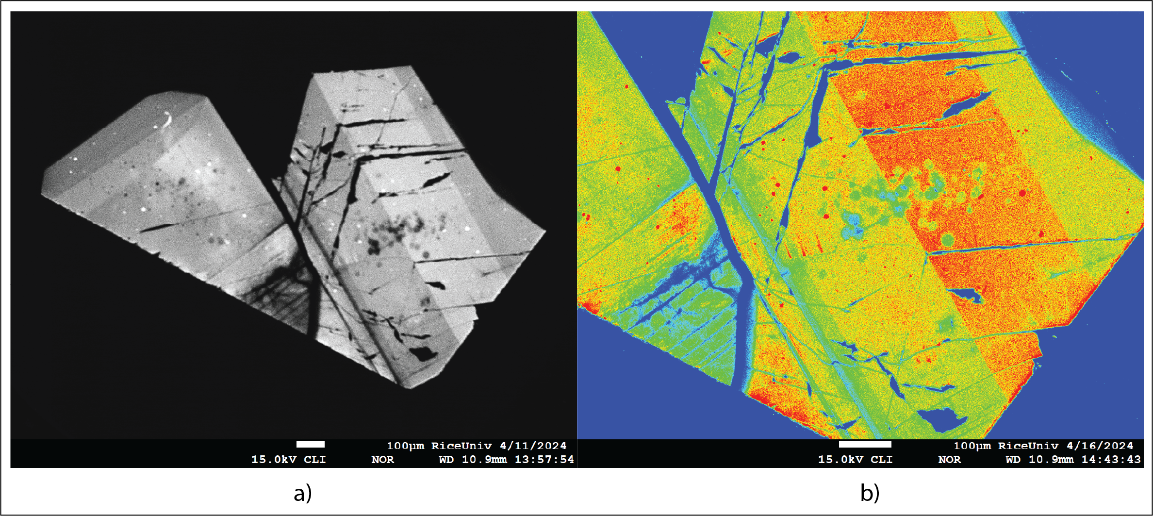
Figure 6. a) CL image of zoned and twinned albite-rich plagioclase (in grayscale); b) The same Albite-rich plagioclase in fake colors.
Other Not-So-Useful Signals in EPMA
- Auger electrons
The secondary electrons produced deeper in the samples do not reach the surface, but they can knock other inner shell electrons and slowly lose their energy through heat. As a result, the sample will get hotter. However, near the surface, the electrons from the outer shell can be knocked out by higher energy secondary electrons and can succeed in leaving the sample. These are called Auger electrons. Auger electrons (always outer shell electrons from the sample) can be also emitted by an atom if a high-energy X-ray kicks out an outer shell electron.
- Heat
A large fraction of the energy of the electron beam is consumed in exciting lattice vibration in the sample and thus produces heat. Heating by the electron beam can sometimes cause “beam damage” in certain samples containing volatile elements, have a low melting temperature, or have a low average atomic number.
Using X-rays for analysis
Semi-quantitative analysis by EDS and WDS
An Energy Dispersive Spectrometry (EDS) detector placed inside the sample chamber (above the sample), can identify and discriminate the emitted x-rays by their energy, as well as it can count the X-rays of different energy. A spectrum with the intensity of the X-rays (number of counts per second) versus the energy of the characteristic X-rays is produced by the EDS analysis. The peaks in the spectrum (the characteristic X-rays) are automatically identified and labeled with the element and the type of X-ray line (e.g. FeKα, Pb Mβ etc.). The height of the peak for the element “i” is proportional with the concentration of the element (i) in the sample, therefore, when the height of the peak is compared to a virtual “100 wt% pure standard”, the concentration of the element “i” can be calculated. By doing this, the identified elements are listed and their concentration (wt%) is calculated. The sum of the elements is usually far from being 100%, but the analysis can be normalized to 100%. This EDS analysis is called “standardless analysis”. However, the elements can also be standardized in the EDS analysis. Prior to the analysis, each element can be analyzed from a known standard. The element “i” in the standard has a known concentration, which is attributed to the measured intensity of the peak for element “i” in the standard. Then, by analyzing the unknown sample, the peak intensity of the element “i” is compared to the real value of the intensity of the element “i” in the standard. By doing so, the measured values (wt%) of the elements are closer to real values (closer to quantitative analysis) and the sum of the measured elements is closer to 100% (without being normalized to 100%).
Our Jeol JXA 8530F hyperprobe has an integrated EDS detector, meaning that a combined quantitative analysis can be performed, where some elements can be analyzed in EDS mode and others in WDS mode.
Quantitative analysis by counting the X-rays (WDS analysis)
The x-rays produced by the sample are detected and counted by several (our probe has 4) wavelength dispersive (WDS) spectrometers, vertically installed around the sample chamber. Each spectrometer contains 2 to 4 (analyzing) crystals and one X-ray detector. Both analyzing crystal and the detector can be moved along a circular path (Rowland circle) and positioned at a desired angle (as determined by Bragg’s equation – Figure 3) to reflect (in fact diffract) a specific x-ray wavelength coming from the sample into the detector (an x-ray counter), while allowing the other wavelengths to be absorbed by the crystal (Figure 4).
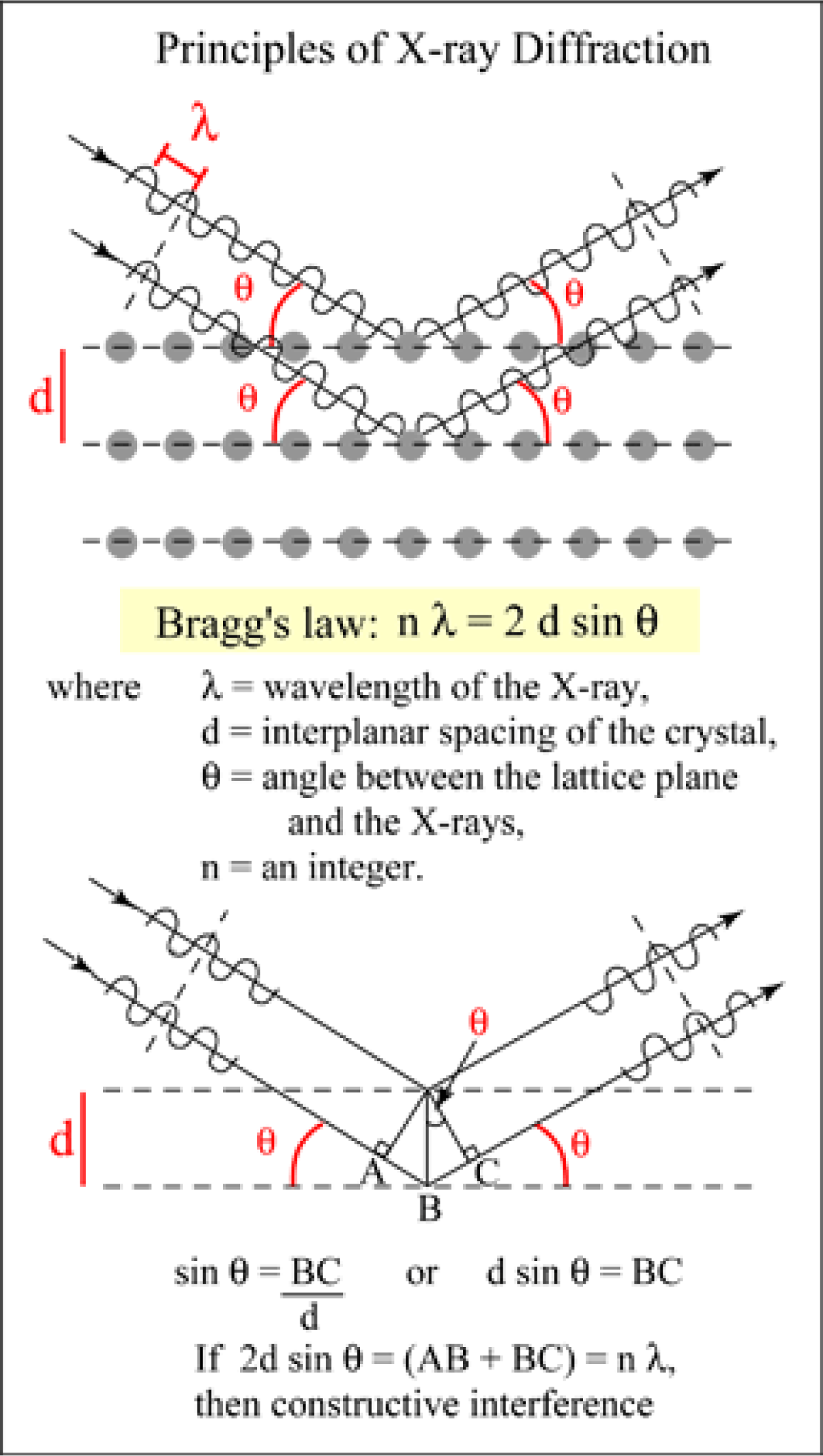
Figure 7: Bragg’s equation, explained
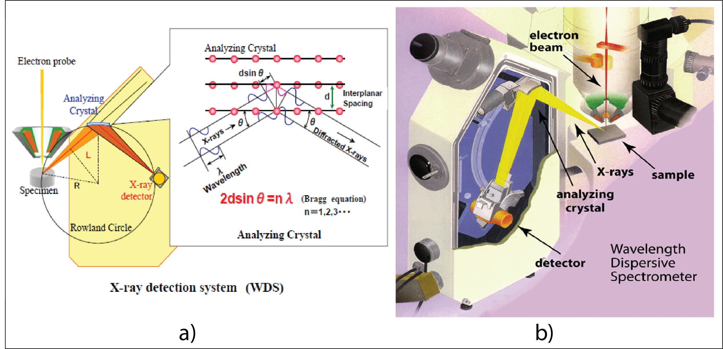
Figure 8. X-ray detection system (WDS); a) Working principle of a Wavelength Dispersive Spectrometer (WDS) in EPMA; b) Sketch of spectrometer showing the position of the analyzing crystal and detector on the Rowland circle.
The intensity of X-rays produced by the element “i” in the sample can be expressed as the number of X-rays counted in one second (counts/sec = cps) by the detector. The wavelength of characteristic X-rays for all elements is known, and so is the sinӨ (where Ө is the angle between the incident electron beam trajectory and the trajectory of the refracted X-ray), as in Bragg’s law.
The Cameca probes operate the spectrometer movement and X-ray indexing based on sinӨ values. The JEOL probes operate with the “L value”, where L is the length of the cord connecting the sample with the analyzing crystal (the length of the refracted X-ray from the sample to the analyzing crystal) or L=2RsinӨ. By construction, R (the radius of the Rowland circle) is 160 mm for Cameca probes, and 140 mm for JEOL probes (except for the “H” spectrometers in JEOL probes, which have R=100 mm). When setting the position of the analyzing crystal to a unique “sinӨ” or “L” value for an element “i”, the analyzing crystal will diffract the X-rays coming from the element “i”, only. This happens because the X-rays which have a wavelength similar to the d interspacing of the analyzing crystal lattice will be refracted, while the rest of the X-rays will be absorbed by the crystal. This is the very principle that made possible the invention of the electron microprobe by the French PhD student Raymond Castaing in 1952. The X-rays produced by the element “i” can thus be counted over a specified length of time (“counting time”). As the crystal of a WDS spectrometer can only collect X-ray counts for one wavelength at a time, the analysis of multiple elements on a single spectrometer must be done sequentially. In addition, no single type of crystal can satisfy Braggs’ Law for the full range of x-ray wavelengths emitted by all the elements in the periodic table. For these reasons, the modern electron microprobes are equipped with more spectrometers, with a “build in” ability to automatically exchange different analyzing crystals within a single spectrometer. Our microprobe has 4 WDS spectrometers containing 10 diffracting crystals which allows us to collect x-ray counts on four elements simultaneously for all elements Z ≥ 4.
How do we get numbers out of X-rays?
Quantitative microprobe analysis is based on the comparison between a) the measured intensity (net cps) of the X-rays of each element “i” present in an unknown sample, and b) the measured intensity (net cps) of the X-rays of the same element “i” in a standard material, where the concentration of each element “i” is known. The comparison is made between the net intensities of the X-rays in the unknown and the standard, where the net intensity (I) is the difference between the total peak intensity (IP) and the intensity of the average lower and upper background (IB).
For any element (i) the net intensity I is I = IP-IB
For any element “i”, the ratio “net Intensity of element “I” in the unknown sample versus the net intensity of the element “I” in the standard” or Iunk/Istandard is known as the k-ratio. Therefore, the concentration of element “i” in the unknown sample (Ciunk) is given as the approximation (known as Castaing’s First Approximation):
Where Iiunk is the net intensity of the X-rays produced by the element “i” in the unknown, Iistd is the net X-ray intensity produced by the same element “i” in the standard, Cistd is the concentration in wt% of the element “i” in the standard and Ki is the k-ratio for element “I”.
For example, if under the same conditions, we obtain the net intensity (I) of 20,000 counts/sec for Fe on an unknown sample and 40,000 counts/sec for Fe on a standard containing 50 wt% Fe, to a first approximation, the Fe content in the unknown sample is calculated as (20,000/40,000) * 50 wt% Fe = ½ * 50 =25 wt% Fe.
Matrix correction
In practice, Castaing’s First Approximation (see above) must be corrected to account for the effects of other elements present in the sample (and standard), which may differentially affect the x-ray production (i.e. matrix effects). The most common matrix correction is called ZAF and it was first proposed by Castaing. It means that our concentration of the element “i” calculated by the first approximation must be multiplied with a ZAF ratio, where:
- Z is a correction factor for different elements with different atomic number Z present in the unknown and the standard
- A is a correction factor for differential absorption of X-rays
- F is a correction factor for the differential generation of secondary fluorescence.
The “Z” correction factor
In the analytical volume (or volume of interaction between the beam electrons and the sample), incident electrons lose energy in inelastic interactions with the inner shell electrons of the sample. A material with a high mean Z has a higher density and a more complex electronic configuration than a material with a lower mean Z. It means that for the same accelerating voltage, the depth to which the beam electrons can penetrate is smaller than the depth of penetration materials with lower mean Z. The so called “stopping power” (energy lost by the beam electrons per unit mass penetrated) is not constant but drops with increasing Z. The coulombic field in materials with higher Z being stronger than in materials with lower Z, will have as a consequence the production of a higher number of backscattered electrons, and accordingly, a lower number of scattering events, therefore, a lower number of X-rays will be produced. This effect can be easily seen when compared the net X-ray intensity produced by a heavy element (e.g. FeKα from Fe metal, analyzed on LiF analyzing crystal) with a net X-ray intensity produced by a lighter element (e.g. SiKα in Si metal on the TAP analyzing crystal). On the other hand, even we have a smaller number of scattering interaction in the materials with higher Z, the more complex electronic shells of the higher Z elements will cause a higher number and a larger family of X-rays (e.g. significant Lα, Lβ, Mα, Mβ) will be produced by Fe, compared to an element with a lower Z. If both Si and Fe are present in the same sample, for an equal concentration of Si and Fe, the number of the X-rays produced would be different, and thus, the result of the first Castaing’s approximation should be corrected for Z. This correction has two components: correction for the “stopping power”and correction for “backscatter”. Since a higher number of X-rays will be produced in higher Z samples, if the mean Z of the unknown is higher than that of the standard, a downward correction in the composition must be applied.
The “A” correction factor
Some of the X-rays generated in the analytical volume don’t get to escape the sample and are absorbed by all elements present to a differing degree, and in all propagation directions. The absorption along the path to the X-ray detectors and the length of that path requires a correction from measured (i.e., emitted) intensity to obtain the initial (i.e., generated) X-ray intensity. This correction is called the absorption correction (A).
The “F” correction factor
X-rays generated by a given element, with an energy close to and higher than the critical excitation energy of another element, in its way out of the analytical volume, may knock out an electron from an outer shell. Since the vacancy created in this way will always be occupied by an electron from an even outer shell, a photon will be emitted, and hence an X-ray will be produced. This phenomenon is known as secondary fluorescence. Therefore, the high energy X-ray of an element “i” fluoresce the X-rays of the other element ”j” and accentuate the X-ray intensity of the element “j” relative to that produced by electron excitation alone. The additional contribution of fluorescence by characteristic X-rays is called F the fluorescence correction.
The parameters for Z, A, and F are typically used to multiply the result obtained by the “castaing’s first approximation”. The so called “ZAF correction” is Z*A*F, aplied for the standards, as well for the unknown.
If the standard material has ZAF numbers identical with the ZAF numbers of the unknown sample, then the effect of the matrix correction will cancel each other (ZAFiunk = ZAFistd). This is why, in practice, we try to choose the standards to be of the same material type as the sample we analyze as unknown.
For example, a microprobe analysis of an olivine MgxFe1-xSiO4 which contains O, Mg, Si, and Fe, it is necessary to correct for the effects of electron retardation and scattering, X-ray absorption, and X-ray fluorescence of all other elements on the element of interest. The emitted X-ray intensities are measured for the Kα lines of Mg, Si, and Fe on an olivine sample, and the k-ratio for each element is calculated relative to the standard used. For an olivine analysis we would use the standards synthetic forsterite for Mg and Si, and synthetic fayalite for Fe, so the emitted X-ray intensities for Mg and Si would be measured on the forsterite standard, and the emitted intensity for Fe on the fayalite standard.
That is, the concentration of Mg in the olivine sample is obtained from the k-ratio for Mg multiplied with the concentration of Mg in the forsterite standard, and all is corrected using the factor ZAF (the result is multiplied with F, A and Z correction factors). It is important to understand that the ZAF factors are a function of composition, so that the conversion from k to C is performed by iterative calculation, matrix inversion and includes many other calculations not discussed here. The analytical approach is very powerful because a minimal set of calibration standards can be used for quantitative analysis of a given element over essentially the entire concentration range from trace element to pure element using the algorithms for the ZAF factors.
Probe diameter (beam size in “spot” setting)
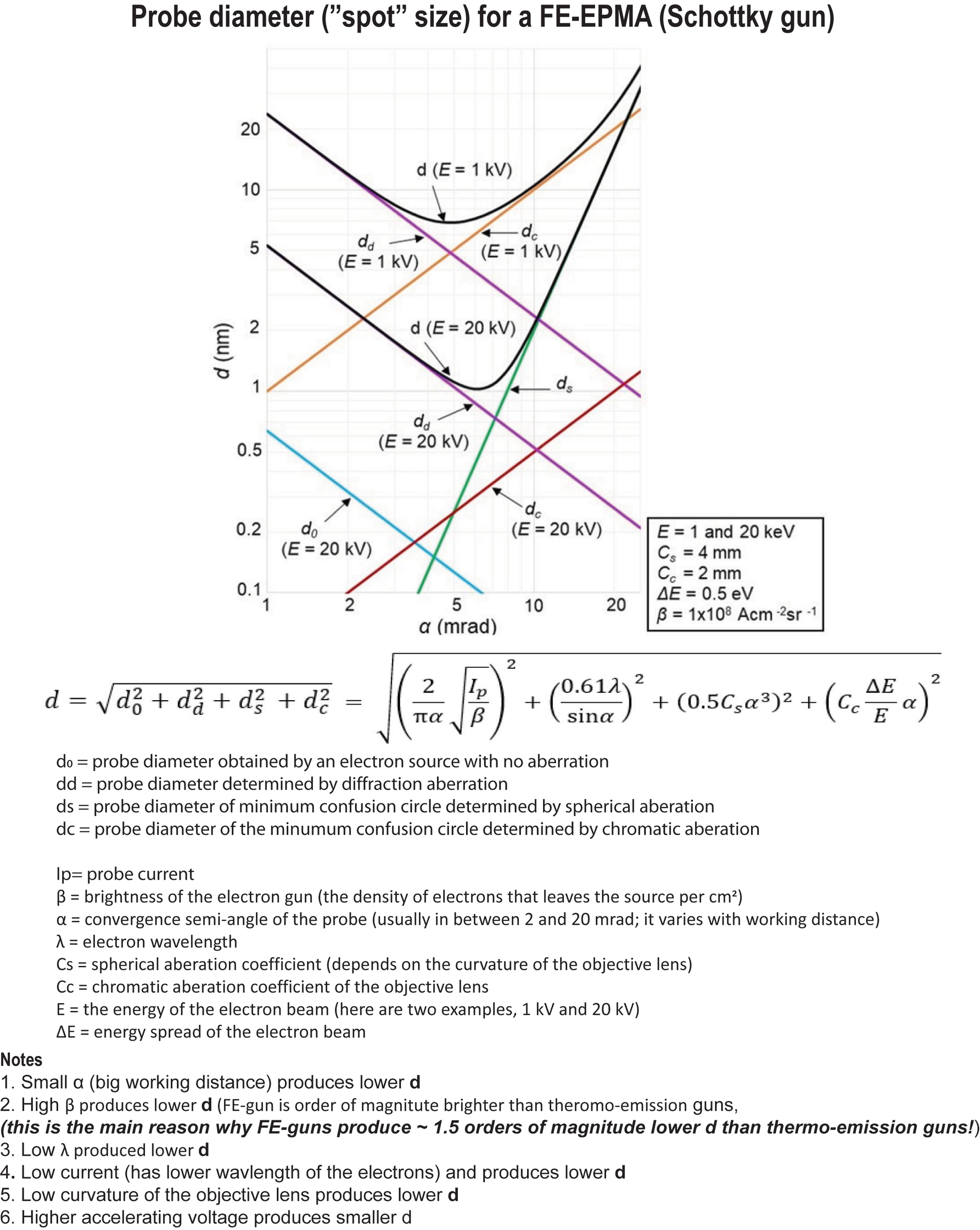
Figure 9: Probe diameter (d): how it is calculated
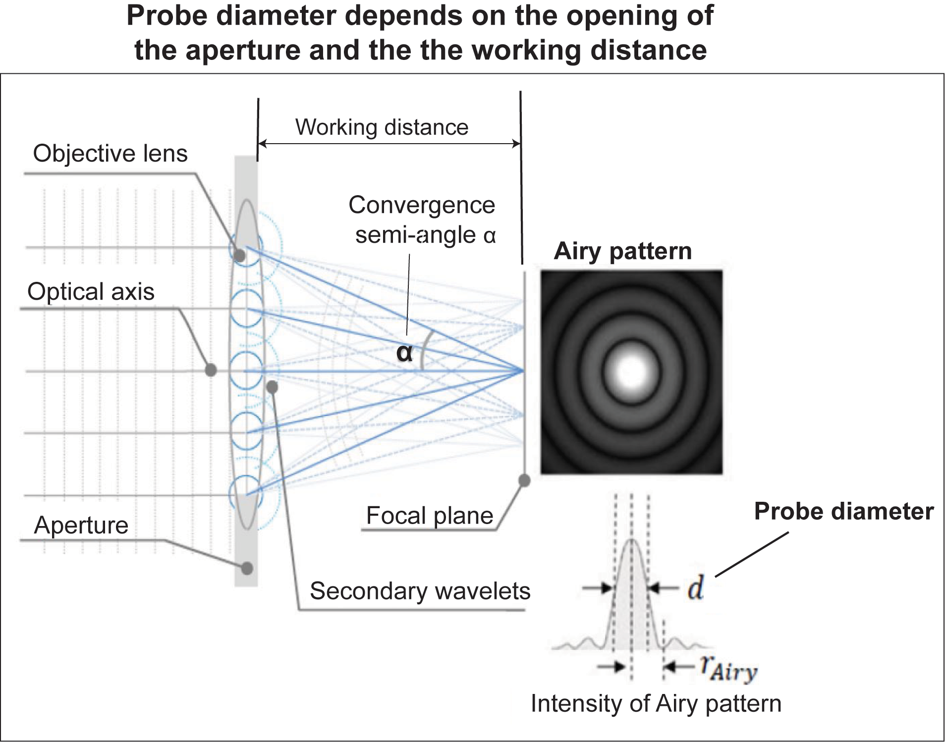
Figure 10: Probe diameter is influenced not only by accelerating voltage and probe current, but also by a) aperture opening, b) working distance, c) convergence semi-angle α, and d) objective lens (giving spherical and chromatic aberration)
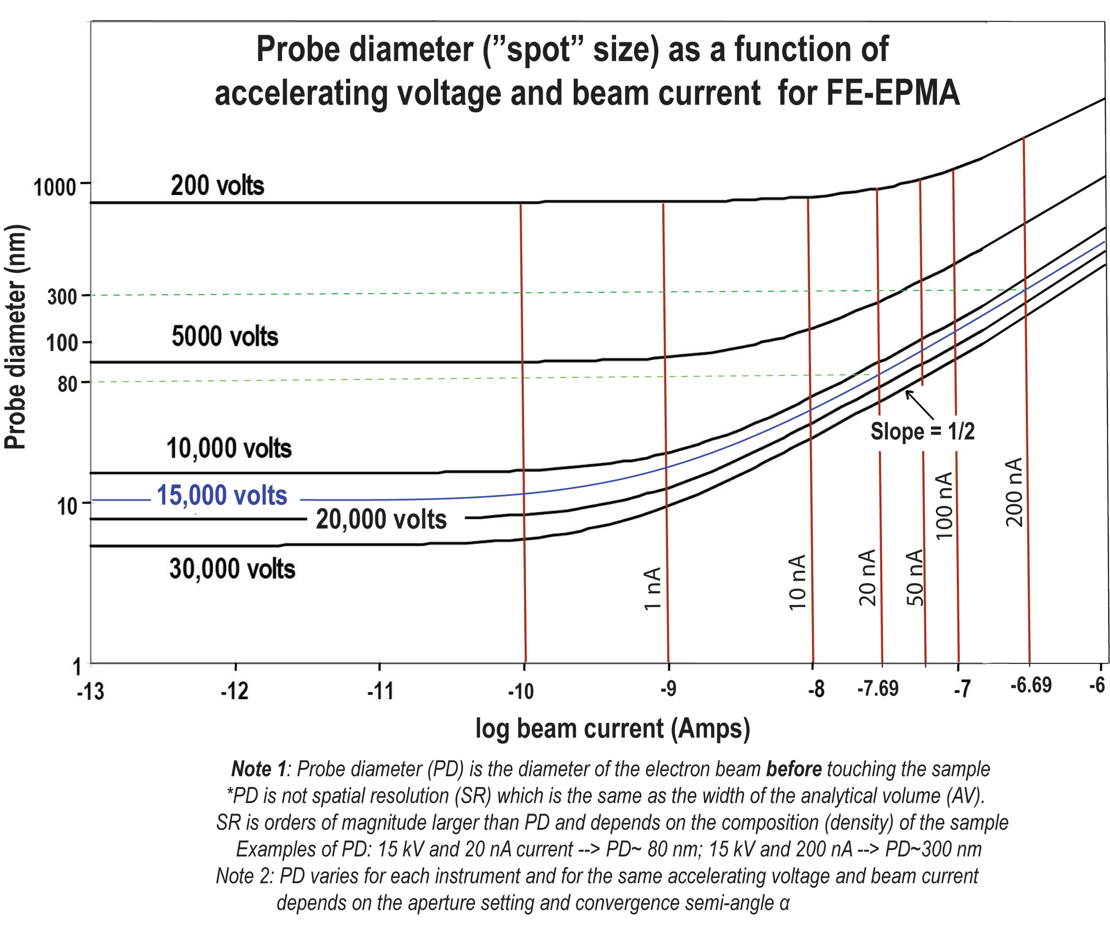
Figure 11. Probe diameter as a function of accelerating voltage and probe current for FE-EPMA (Schottky gun)
About the lab: EPMA configuration and capabilities
Contact
Dr. Gelu (Gabi) Costin
EPMA Lab Manager
Department of Earth Science
Rice University
6100 Main Street, Keith-Wiess Geological Laboratory, MS-126
Houston, TX, 77005
e-mail: g.costin@rice.edu Phone: Office: 713 348 2054
